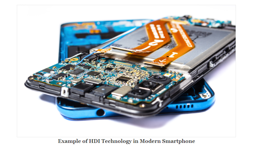
HDI PCB technology has been a major enabler of advancement in the electronics industry, providing the dense interconnections and intricate circuitry needed to push the boundaries of miniaturization and functionality. From wearable consumer devices to industrial, military and aerospace systems, HDI PCB technology has allowed the use of advanced heterogeneous 2.5D and 3D semiconductor packages that drive many of them the smaller, faster, and more functional devices we enjoy today.
However, the production and assembly of HDI PCBs come with unique challenges. Achieving intricate high-precision conductive patterns and traces that function reliably and efficiently requires specialized manufacturing capabilities, particularly when PCB layer counts are high (greater than 10).

In my work at PCB Trace Technologies, we recently manufactured a 20-layer HDI PCB for a commercial aerospace company. We used a modified semi-additive process (mSAP) as an alternative to subtractive etching to form the conductive circuit patterns. This approach offered better pattern geometry, allowing for finer traces and tighter spacing, as narrow as 3 mil (0.075 mm).
As a PCB fabricator that has developed expertise and capabilities in HDI technology, we can provide a summary of best practices to help others in the industry successfully navigate the complexities of designing and fabricating HDI circuitry.
HDI guidelines and standards
There are four IPC standards concerning HDI PCBs that collectively provide guidance on HDI PCB design and manufacturing. Following these guidelines and standards provides many advantages, from improved efficiencies and process controls to enhanced product quality and customer satisfaction.
● IPC-2315, called the HDI Design Guideline, outlines design recommendations for HDI PCBs
● IPC-2226 serves as an extension of generic guidelines for PCB design (IPC-2221) and provides in-depth standards and guidance for HDI PCB design
● IPC-4104 specifies material sets that are appropriate for HDI PCBs, covering the various conductive and dielectric materials that can be used
● IPC-6016 is another design qualification standard for HDI PCBs.
Design considerations for HDI circuits
Designing HDI PCBs necessitates careful consideration of several factors to ensure optimal performance, functionality, and reliability.
● Plan meticulously for layout and placement of components. That way, you will make the most of limited board real estate while preventing signal interference. This includes selecting the right package types and strategically locating critical components.
● Keep careful track of minimum trace widths and spacing, which can be incredibly narrow. HDI PCBs commonly feature trace and space widths in the range of 2 mils (0.002 inches) or smaller.
● Pay attention to impedance control, as HDI circuits often handle high-speed signals. Proper impedance matching and controlled trace geometries are crucial to minimize signal reflections and losses.
● Carefully consider thermal management. It’s important because of higher component density, processing power and speed in HDI boards. Effective heat dissipation strategies, including the use of thermal vias and copper pours, are essential to prevent overheating and ensure long-term reliability.
● When selecting materials, consider material characteristics, such as dielectric constant, thermal properties and mechanical strength. All materials used to fabricate and assemble the HDI PCB can significantly impact signal performance and board reliability, especially the choice of substrate material.
● Optimize for fewer layers. Boards with higher layer counts require more assembly steps and increase manufacturing costs.
Vias in HDI PCBs
HDI PCBs use multiple types of vias to make vertical electrical connections. Choose via types and placements wisely. Each serves a unique purpose and influences routing density and signal integrity.

● Through-hole vias (THVs) traverse the entire thickness of the board, allowing electrical connectivity between top and bottom layers. THVs are well-suited for most applications, including high-power designs. They are also preferrable with large components with pin leads such as connectors, where mechanical strength and reliability are paramount.
● Blind vias connect an outer layer to one or more inner layers, without traversing the entire PCB. They are constructed by means of mechanical or laser drilling, depending on the hole diameter.
● Buried vias link inner layers without extending to the board’s surface. They are also constructed by means of mechanical or laser drilling, depending on the hole diameter.
● Microvias are used in very dense, high-layer count boards. They have diameters smaller than 6 mils and must be laser drilled.
● Via-in-pad places vias directly under surface-mount component solder pads, instead of routing the trace around the pad. Via-in-pad requires filling and capping to prevent solder from wicking through to the back layer of the PCB.
Via plating
Traditionally, electroless copper plating was the preferred method for plating via holes in PCBs. While the electroless copper process is well-established and known for its reliability in creating interconnects, it consumes large amounts of water and energy, uses toxic chemicals and is a significant source of hazardous waste, raising serious environmental and health concerns.
Recently, innovative alternatives to electroless copper plating, called direct metallization, have emerged. Compared to electroless copper plating, direct metallization provides shorter cycle times and improved hole wall reliability, while dramatically reducing chemical and water usage, energy consumption, costs, and the carbon footprint.
Future of HDI
Globally, the HDI PCB market value of $8.2 billion in 2022 is expected to grow to $11.3 billion by 2028. This growth reflects a promising opportunity for PCB fabricators. People who embrace the trend for smaller, sleeker and more functional devices will become agile leaders in HDI technology that can help customers push the boundaries of miniaturization in next-generation electronics.
About US
Heisener Electronic is a famous international One Stop Purchasing Service Provider of Electronic Components. Based on the concept of Customer-orientation and Innovation, a good process control system, professional management team, advanced inventory management technology, we can provide one-stop electronic component supporting services that Heisener is the preferred partner for all the enterprises and research institutions.