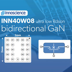
Innoscience Technology has released a 40V bidirectional Gan-on-SI enhanced mode HEMT called INN40W08, which uses the company's advanced InnoGaN Technology to provide ultra-low resistance. For mobile devices, laptops and phones.
Dr Denis Marcon, General Manager of Innoscience Europe and Marketing Manager for THE US and Europe, commented: "GaN technology has been adopted by mobile phone charger manufacturers in the past few years to provide greater power and reduce device size. However, Innoscience's major breakthrough now makes it possible to introduce GaN Hemt into mobile phones, improving efficiency and performance. With Innoscience's vast available capacity, we can deliver the secure supply chain that our customers now expect."
The new GaN HEMT provides bidirectional blocking capability, providing an ultra-low on-resistance of just 7.8mOhm. The company's advanced InnoGaN provides this patented strain enhanced layer technology that reduces thin layer resistance by 66%. The gate charge (QG) is usually 12.7nc. The 5x5 grid WLCSP is only 2mm x 2mm in size. This small size allows these GaN Hemts to be integrated inside the phone. Applications include high-end load switches, overvoltage protection in smartphone USB ports, multiple power supplies, and chargers and adapters.
The company's GaN technology promotes efficient and more compact OVP systems by replacing two silicon MOSFets with a single InnoGaN (or BiGaN) transistor. This saves overall OVP costs and makes the unit smaller, which is extremely important given the space constraints on the phone's circuit board.