Electronic engineers and technicians are accustomed to seeing noise as a negative factor and therefore optimize for low noise during component selection, circuit design, and circuit board layout. In fact, random or pseudo-random noise can sometimes be useful. This article will further explain why and how to use noise.
Electronic engineers and technicians are accustomed to seeing noise as a negative factor and therefore optimize for low noise during component selection, circuit design, and circuit board layout. In fact, random or pseudo-random noise can sometimes be useful. This article will further explain why and how to use noise.
In various applications, there are two types of random noise commonly used: white noise and pink noise. White noise has a relatively flat spectrum with the same bandwidth power (measured in dB). Pink noise has the same power at every frequency octave within its bandwidth (Figure 1).
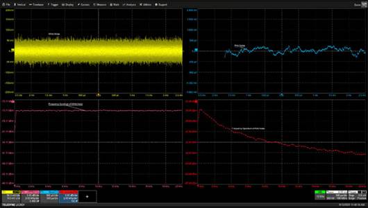
Figure 1: Spectrum comparison of white and pink noise. The power spectrum of white noise is flat, while that of pink noise decreases by 3 dB per octave
Pink noise can be used in audio testing and sound system equalization because of its similar response to the human ear.
Room equalization adjusts the frequency response of the sound system to produce the exact same signal as the input signal. If pink noise is input into the sound system, the equalizer will output pink noise after adjusting the measured value on the spectrum analyzer (Figure 2).
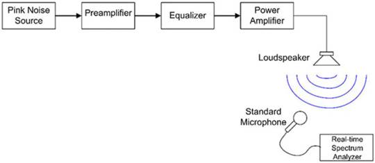
The input can be reproduced without loss or distortion by adjusting the frequency response of the room with an equalizer
White noise can be used to measure frequency response and as a spread spectrum source in spread spectrum communication.
The following example depicts the frequency response of a 10.7 MHz intermediate frequency (IF) filter (Figure 3)

Figure 3: Measurement of the frequency response of a 10.7 MHz IF filter using wideband white noise
As shown in the upper left grid, white noise is fed into the filter through an appropriate impedance matching network. As shown in the bottom left grid, the spectrum of the input noise is flat over the entire target frequency range. The output of the correctly terminated filter is shown in the upper right grid. This output has a smaller amplitude than the input because the bandpass filter attenuates the frequency component outside the filter bandwidth. The spectrum of the filter output (as shown in the lower right grid) shows that the filter has a bandwidth of about 400 kHz at a 10.7 MHz center frequency. The theoretical frequency response is the complex ratio of the output signal to the input signal. Since the amplitude of the input signal is uniform, the output spectrum shows the amplitude spectrum response of the filter.
Construct noise generator
Noise generators can be based on any of the following three basic technologies. The first technique uses Johnson noise produced in a resistor. This electronic noise is produced by the thermal perturbation of electrons inside the conductor, which occurs at any voltage. The resulting noise is essentially white Gaussian noise, which must be buffered by some ultra-high gain amplifier.
The second technique is to use reverse bias Zener diodes or avalanche breakdown diodes. This noise is also white noise, and at a higher noise level than Johnson noise, but still requires a high-gain amplifier.
The third technique uses shift registers to generate pseudo-random binary sequences (PRBS), which are then converted into white noise using digital-to-analog converters (DAC) and filters. PRBS noise streams have a finite repetition length. The length can be set by the order of the shift register. The reciprocal of the signal duration is the lowest frequency that the PRBS generator can reproduce. PRBS generators provide the highest output voltage and do not require high gain amplifiers.
The PRBS generator can be implemented using a discrete shift register (see Figure 4) or a programmable system-on-chip (such as a microcontroller or FPGA).

A 16-bit PRBS noise generator is realized by using two discrete eight-way D-type flip-flop ics
The PRBS generator (see Figure 4) is a low-cost, linear feedback shift register implementation using onsemi's MC14015DG dual 4-bit static shift register and Texas Instruments' CD4070BMT four-way XOR gate. 16 way Type D trigger (8 way per IC) has feedback taps in 14th and 15th way to produce PRBS15 data mode. The feedback connection is made through an XOR gate. The data mode is 32767 bits long and lasts about 65 milliseconds (ms) at a 500 kHz clock rate. Longer patterns can be achieved by using more shift registers and changing the feedback taps appropriately.
Using MC14093BDR2G Schmidt flip-flop with non-gate (IC5) and basic resistance capacitance (RC) network, the generator is initialized to an "all zero" state when turned on. The clock is provided by a simple CMOS oscillator running around 500 kHz. The digital output can be taken from any shift register Q output. In this example, Q14 is used.
While analog filters can be used, they are limited to specific clock frequencies. By using a finite impulse response (FIR) low-pass digital filter, the filter cutoff frequency will track any change in the clock frequency. In addition, FIR filters can provide very low cutoff frequencies, which for analog filters require capacitors with a large capacity. The FIR filter combines the weighted sum of the shift register output. The weighting required to produce a rectangular low-pass filter response in the frequency domain is sin(x)/x in the time domain (Figure 5)

Figure 5: The output stage of the generator uses sin(x)/x weighted samples from the shift register output to implement the FIR low-pass filter
The weighted shift register output is summed over a differential amplifier containing the three parts of a LM324KDR four-channel operational amplifier. The upper resistor group represents the negative value of the sin(x)/x weight. The lower resistor group represents a positive value. This digital filter band limits the output to about 5% of the 500 kHz clock frequency (or 25 kHz) and is suitable for audio testing purposes.
The generator's white noise output can be converted to pink noise using a simple resistance-capacitance filter (Figure 6).

Figure 6: This simple RC filter will use the digital noise output of the generator to produce pink noise
Choose an amplifier that matches the expected load. This type of noise generator is suitable for audio testing and balancing.
| 零件编号 | 描述 | |
|---|---|---|
| MC14046BFEL ON Semiconductor |
时钟/计时 - 时钟发生器,PLL,频率合成器, IC PHASE LOCKED LOOP 16SOEIAJ | RFQ |
| MC14046BF ON Semiconductor |
时钟/计时 - 时钟发生器,PLL,频率合成器, IC PHASE LOCKED LOOP 16SOEIAJ | RFQ |
| MC14046BCPG ON Semiconductor |
时钟/计时 - 时钟发生器,PLL,频率合成器, IC PHASE LOCK LOOP CMOS 16DIP | RFQ |
| MC14046BDWG ON Semiconductor |
时钟/计时 - 时钟发生器,PLL,频率合成器, IC PHASE LOCKED LOOP 16-SOIC | RFQ |
| MC14046BDWR2G ON Semiconductor |
时钟/计时 - 时钟发生器,PLL,频率合成器, IC PHASE LOCK LOOP CMOS 16SOIC | RFQ |
Traction inverters are the main battery drain components in electric vehicles (EVs), with power levels up to 150kW or higher. The efficiency and performance of traction inverter directly affect the driving range of electric vehicle after a single charge. Therefore, in order to build the next generation of traction inverter systems, silicon carbide (SiC) field effect transistor (FET) is widely used in the industry to achieve higher reliability, efficiency and power density.
Do you know the 8 application circuits of operational amplifiers?
This technical presentation requires an understanding of how to configure an operational amplifier in a typical gain control circuit. The applications of linear and nonlinear digital potentiometers are discussed. This article gives an overview of the basic techniques required to convert audio and other potentiometer/op amp applications from conventional mechanical potentiometers to solid state potentiometers
The current in an electronic circuit usually has to be limited. In USB ports, for example, excessive current must be prevented to provide reliable protection for the circuit. Also in the power bank, the battery must be prevented from discharging. Too high discharge current results in too large voltage drop of the battery and insufficient supply voltage of downstream devices
Using advanced real-time control technologies such as motor control circuits with higher power density, higher integration and more efficient systems, better acoustic performance of the system can be achieved
Brushless direct current (BLDC) motors have been widely used in household appliances, industrial equipment and automobiles. While brushless DC motors offer a more reliable and maintainable alternative to traditional brushless motors, they require more sophisticated electronics to drive them
How to achieve precise motion control in industrial actuators
The NCP51820 is a 650 V, high-speed, half-bridge driver capable of driving gallium nitride (" GaN ") power switches at dV/dt rates up to 200 V/ns. The full performance advantages of high voltage, high frequency and fast dV/dt edge rate switches can only be realized if the printed circuit board (PCB) can be properly designed to support this power switch. This paper will briefly introduce NCP51820 and the key points of PCB design of high performance GaN half bridge grid driver circuit using NCP51820