The CY29973 has an integrated phase-locked loop, which provides low tilt and low jitter clock output for high-performance microprocessors. Three independent four-group outputs and one independent phase-locked loop feedback output FB_ OUT provides extremely high flexibility for possible output configurations. Since VCO is configured to operate between 200 MHz and 480 MHz, PLL can ensure stable operation.
Logic Block Diagram

This allows a wide range of output frequencies up to 125 MHZ. The phase detector compares the input reference clock with the external feedback input. In normal operation, the external feedback input FB_IN is connected to the feedback output FB_OUT. The internal VCO runs on multiples of the input reference clock set by the FB_SEL(0:2) and VCO_SEL select inputs
Synchronous output
The SYNC output provides a signal for system synchronization in cases where the output frequency relationships are not integer multiples of each other. CY29973 monitors the relationship between the QA and QC output clocks. It provides a low pulse with a duration of one cycle, one cycle before the consistent rising edge of QA and QC output. The duration and location of the pulse depends on the higher of the QA and QC output frequencies. The following sequence diagram illustrates the various waveforms that SYNC outputs. Note that the SYNC output is defined for all possible combinations of QA and QC outputs, even though under some relationships the low frequency clock can be used as a synchronization signal.
Synchronous output with different input and output ratios

The VCO frequency is then divided into the desired output frequency. These dividers are selected by SELA(0,1), SELB(0,1), SELC(0,1) for input Settings.For cases where the VCO needs to operate at a relatively low frequency and may therefore be unstable, assert VCO_SEL low to divide the VCO frequency by 2. This preserves the desired output relationship, but provides an enhanced PLL lock range.
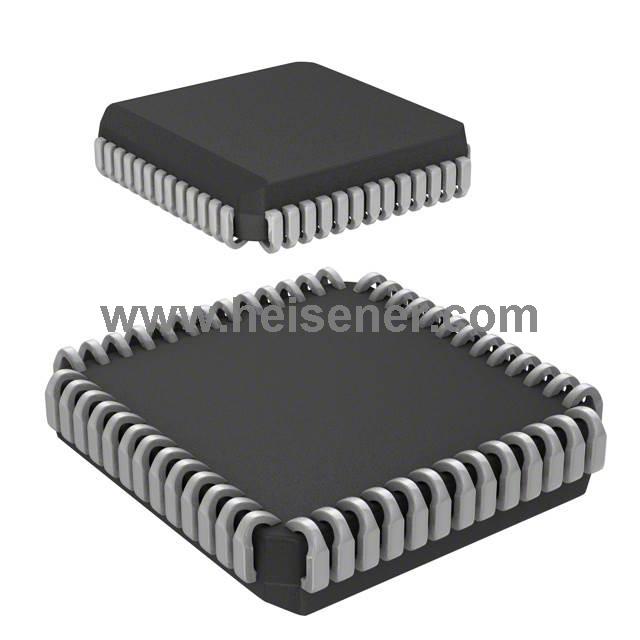
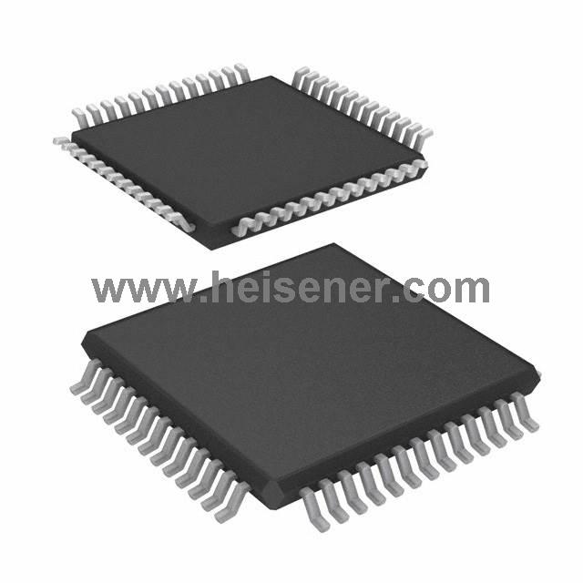
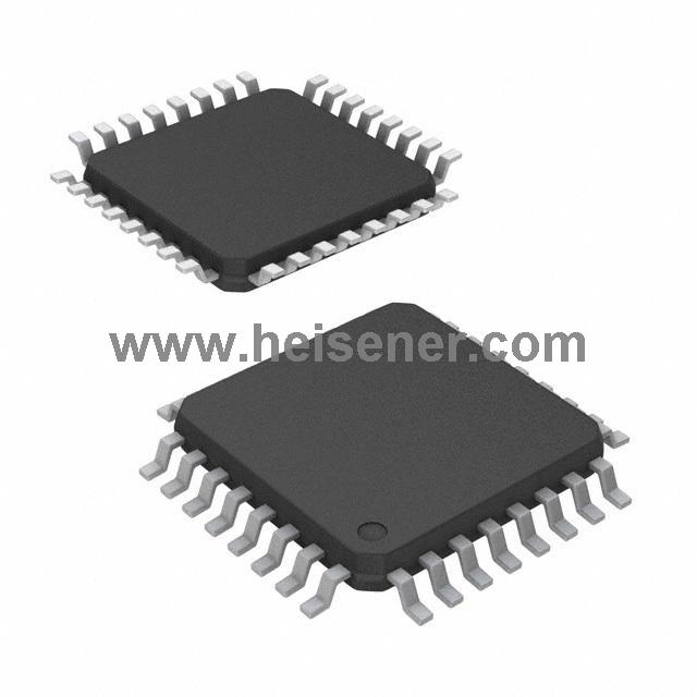
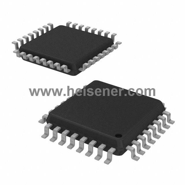
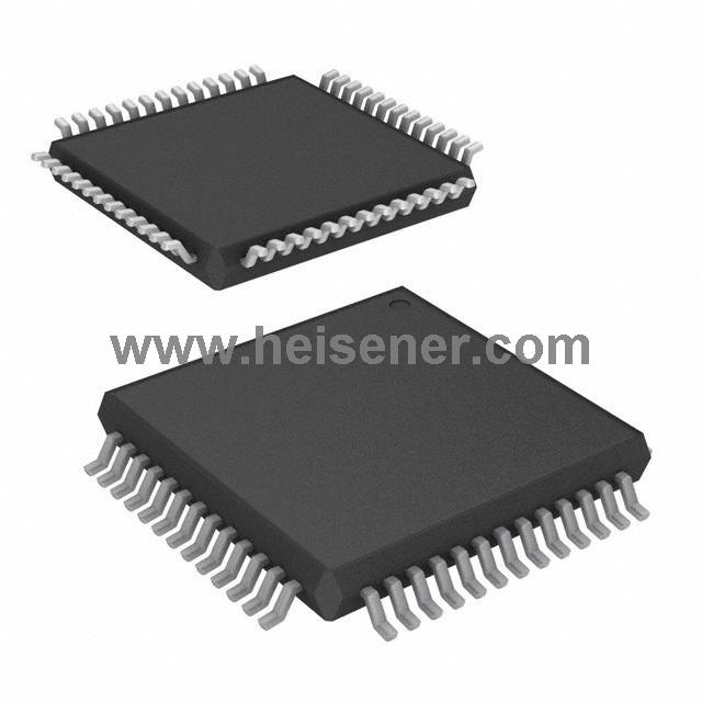
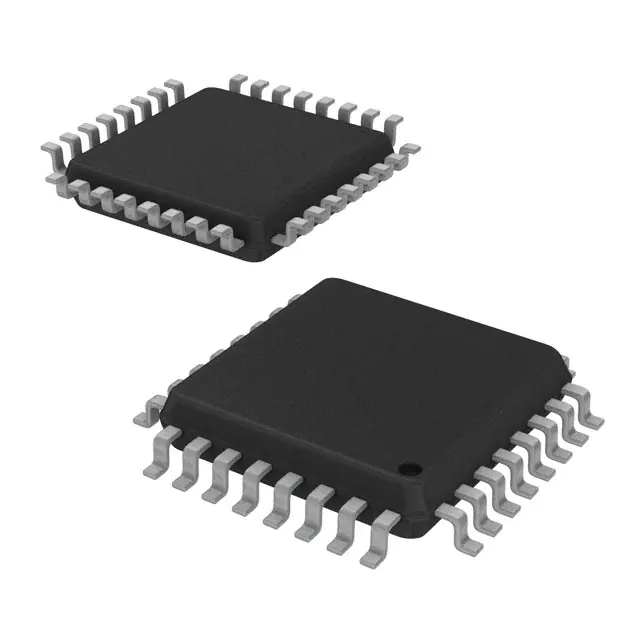
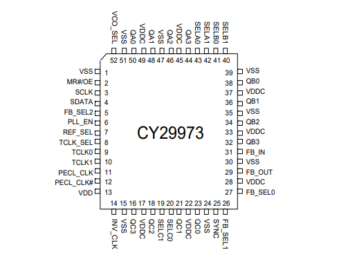
Pinouts
The CY29973 is also capable of providing a reverse output clock. QC2 and QC3 output clock reversal when INV_CLK is asserted to be high. These clocks can be output as feedback to the CY29973 or a second PLL device to generate early or late clocks for specific designs. This inversion does not affect the output-to-output skew
Features
● Output Frequency up to 125 MHz
● 12 Clock Outputs: Frequency Configurable
● 350 ps max. Output to Output Skew
● Configurable Output Disable
● Two Reference Clock Inputs for Dynamic Toggling
● Oscillator or PECL Reference Input Spread Spectrum Compatible
● Glitch-free Output Clocks Transitioning
● 3.3V Power Supply
● Pin Compatible with MPC973
● Industrial Temperature Range: -40 °C to +85°C
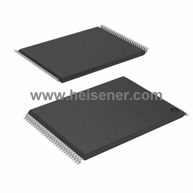
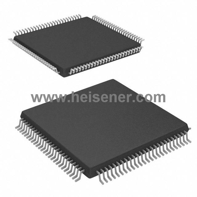
● 52-Pin TQFP Package