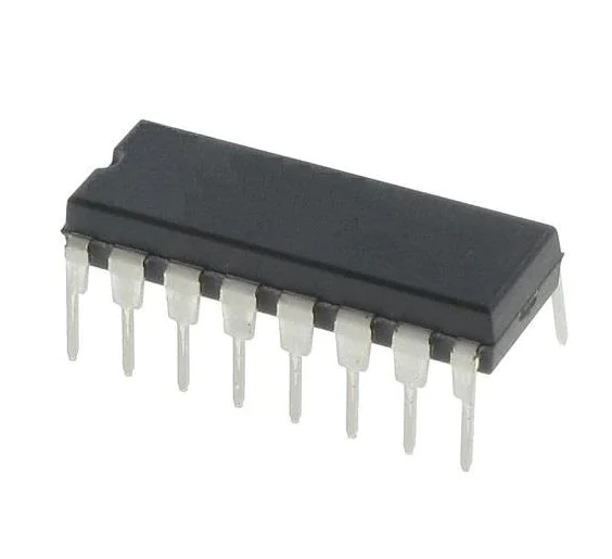
The MM74HC259 device uses advanced silicon gate CMOS technology to implement an 8-bit addressable latch designed specifically for general-purpose storage applications in digital systems. MM74HC259 has one data input (D), eight latched outputs (Q1-Q8), three address inputs (a, B, and C), one public enable input (G), and one public CLEAR input.
To operate the device as an addressable latch, data is stored on input D and the addresses of latches to which data is to be entered are stored on input A, B, and C. When ENABLE is set to LOW, data flows to the addressed output. When ENABLE switches from low to high, data is stored.
All unaddressed latches will not be affected. If this function is enabled in the HIGH state, the device is desselected and all latches remain in the previous state, unaffected by data or address input changes. To eliminate the possibility of entering incorrect data into the latch, the enable should remain HIGH(inactive) when the address row changes.
If enable is kept HIGH, CLEAR is set to LOW, and all eight latches are cleared to LOW. If enable is LOW, all latches except the addressing latches will be cleared. The addressed latch will follow the D input, effectively implementing the 3-8 line decoder. All inputs are protected due to the static discharge of the diodes to the VCC and ground.
MM74HC259 Connection Diagram

MM74HC259 Logic Diagram

Features
● Typical propagation delay: 18 ns
● Wide supply range: 2 -- 6V
● Low input current: 1 µA maximum
● Low quiescent current: 80 µA maximum (74HC Series)