Multiplexed SAR ADCs are typically used in applications that require continuous monitoring of multiple critical variables in a system. In optical communication applications, laser bias can be monitored through optical power measurements, while in VSM applications EEG/ECG signals from electrodes can be monitored. These multiplex applications have some common requirements:
● There are many channels to monitor. In general, an ADC monitors all channels sequentially.
● Channel voltages are usually independent of each other.
● There are strict limitations in terms of system size and power consumption.
Because of these requirements, designers face some challenges. When the ADC completes the conversion on a channel, the sampling capacitance in the ADC is charged to that channel voltage. If the voltage of the sampling capacitor differs significantly from the voltage of the next channel in the sequence, it must be designed through the signal chain so that the sampling capacitor can be accurately stabilized at the new voltage for the allowed sampling time. In the past, a wideband drive amplifier was usually used to solve this problem with an RC filter. A typical signal chain is shown in Figure 1.
Figure 1. Signal chain using traditional multiplexed SAR ADC

The sensor can output voltage or current, and the sensor interface circuit can be an instrumentation amplifier or a mutual impedance amplifier, respectively. Capacitors are usually NP0/C0G because other types of capacitors cause significant distortion. NP0 capacitance has high linearity but low density. The selected NP0 capacitor is also much larger than the value of the sampling capacitance inside the ADC. It performs two key functions:
● Reduce the recoil of the ADC sampling capacitance
● Noise beyond the required stable bandwidth is filtered, thereby reducing the broadband noise of the signal chain
In a traditional signal chain, each channel must use a drive amplifier and a large capacitor. The power consumption of each drive amplifier is between a few tenths of a milliamp and a few milliamps. Each capacitor (including the gap) may occupy about 1mm2 of the board area. If multiple channels use this signal chain, it will be very unfavorable to reduce the size of the system and reduce power consumption. This is one of the major problems in multiplex SAR ADC applications today.
What is input high resistance technology?
In the case of analog inputs, high-resistance technology refers to a set of circuit technologies that substantially increase the effective input impedance of an ADC without consuming static or continuous power. This makes the input to the ADC easy to drive.
Assuming that the multiplexed ADC is converting on channel N-1, the next channel to be converted is channel N.
At the rising edge of the conversion start (CNV), the channel voltage is sampled. In Figure 2, the first rising edge of the CNV samples the voltage of channel N-1. The ADC then converts the sampled voltage across the channel N-1. After conversion, with the input high resistance disabled, the ADC continues to acquire the next channel in the sequence, which is channel N. The voltage on channel N is usually very different from the voltage on channel N-1, at which point the ADC capacitor is charged to reach the voltage level of channel N. This creates a large voltage shock across channel N (dark blue dashed line) and introduces a large error in the channel voltage at the moment of sampling (the second rising edge of the CNV). A large external capacitor is therefore required to absorb the shock, and a drive amplifier is required to provide the necessary charge.
Figure 2. Phase of the AD4696 with the high resistance function enabled and disabled

When the input high resistance is enabled, the ADC's internal sampling capacitance is charged to the current voltage level of the channel to be sampled, and the actual voltage sampling begins. Immediately after the conversion on channel N-1, a high-resistance phase is introduced to precisely charge the ADC sampling capacitor to the current voltage level of channel N. This means that when the ADC sampling capacitor is connected to an external input, it does not provide any charge and does not cause any recoil. In practice, there is usually a small residual error due to charge injection (the first charge shock) of the internal switch. This small residual error makes the stability error of the instantaneous sampling of channel N almost negligible. When the high resistance is enabled, this charge error will significantly improve the stable dynamics of the system.
When the sampling of channel N is complete, the ADC must proceed with the conversion. Therefore, the internal switch disconnects the ADC's sampling capacitance from the external input. Since the switch is on charge injection, this causes a second charge shock. Under normal circumstances, the second charge shock has a longer stability time, so the amplitude of the first charge shock determines the stability error of the channel. Therefore, the amplitude of the first charge shock must be reduced as much as possible.
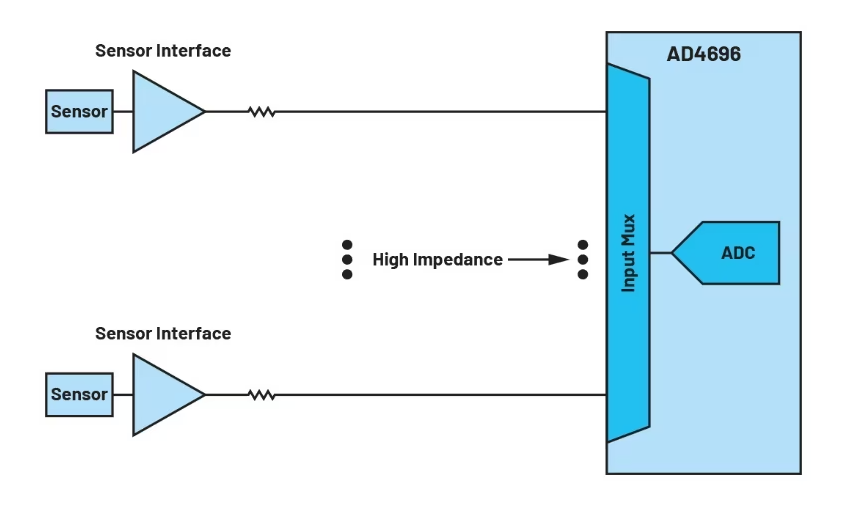
The AD4696 (the next generation multiplexed SAR ADC) incorporates input high resistance technology as part of the EasyDrive™ feature set. As a result, the AD4696 is very smooth when starting voltage sampling on the channel. Each channel no longer requires a recoil absorption capacitor and drive amplifier. This results in a significant reduction in system size and power consumption, and a significant simplification of the signal chain, as shown in Figure 3.
Figure 3. Signal chain using AD4696 multiplexed SAR ADC
An important advantage of achieving high input resistance in the AD4696 series is that the circuits that perform the high resistance function can be cyclically powered on at the conversion rate. Therefore, the power consumption of the high-resistance function will be linearly proportional to the throughput of the ADC, as is the case with the core SAR ADC itself. This is significantly more flexible than the rigid traditional signal chain design.
Input high resistance is also built into the LTspice model of the AD4696. The first and second charge shocks are accurately modeled, making it possible to reliably simulate stable artifacts in the signal chain design.
Some details
A review shows that the NP0 capacitor also provides broadband noise filtering of the signal chain. If you want to remove this capacitance, you have to find other ways to filter out the noise. A simple way to achieve the same effective signal chain noise bandwidth is to increase the external series resistance. The AD4696 has a 60pF internal capacitor in series with a typical 240Ω internal resistor. By setting the external resistance, the signal chain noise bandwidth can be adjusted to the target value.
In the absence of an NP0 capacitor, the external resistance plays an important role in the noise performance, linearity, and accuracy of the signal chain. A small resistance helps to sample charge shock quickly and stably, which improves linearity and accuracy, but a higher effective noise bandwidth results in an overall increase in noise. In contrast, a large resistance can better filter out noise, but linearity and accuracy will be reduced.
As described in the following section, the main advantage of the AD4696's high resistance technology is that it allows for the use of large resistance resistors (thus enabling better noise filtering) without any loss of linearity or accuracy. It enables optimization of all parameters in the signal chain, including noise, linearity, accuracy, power consumption, and solution size.
Measurement result
In the absence of any NP0 capacitance, the measurement is made with a 2kΩ external resistor. The results show that AC and DC performance is significantly improved with the analog input high resistance enabled. The AD4696's core ADC was run at 1MSPS, but more channels were selected as part of the polling sequence. The data is collected on one channel, and the input voltage of the other channels in the sequence is 0V.
Figure 4. Relationship between THD and the number of channels in the sequence. Test tone: 1kHz, - 1dBFS

Figure 4 shows the distortion performance of the relevant channel at 1kHz, -1dBFS signal tones. When channels are sorted with high resistance disabled, a nonlinear stabilization error occurs because the sampling capacitor is not charged to the voltage level of subsequent channels. This can cause serious distortion. After the high resistance is enabled, the distortion performance is greatly improved.
Figure 5.DC stabilization error in the 16-bit level LSB

Figure 5 shows the DC steady-state setup error with and without the high-resistance function. In this test, the relevant channel has an input value near full scale, and the other channels in the sequence are driven at a voltage of 0V. Transformations are made on the relevant channels while more and more channels are added to the sequence and the offset of the average output code from the expected code is plotted.
When the core ADC is running at throughput below 1MSPS, users may need to further reduce the effective signal chain noise bandwidth to limit analog front-end noise aliasing. This will require higher resistance values, and the high resistance feature is very helpful in maintaining performance under these conditions.
Conclusion
The AD4696 series uses input high resistance technology to provide significant benefits for multiplex SAR applications, such as reduced system-level power consumption, reduced size, and reduced component count, while maintaining a high level of AC performance and DC accuracy. This eliminates the need for dedicated drive amplifiers and recoil absorption capacitors for each channel. The power consumption of the high-resistance function itself is proportional to the throughput of the ADC, providing good flexibility and versatility for system-level design. The LTspice model of the AD4696 can be used to simulate the effects of charge shock in any system the user wishes to design.
Heisener Electronic is a famous international One Stop Purchasing Service Provider of Electronic Components. Based on the concept of Customer-orientation and Innovation, a good process control system, professional management team, advanced inventory management technology, we can provide one-stop electronic component supporting services that Heisener is the preferred partner for all the enterprises and research institutions.