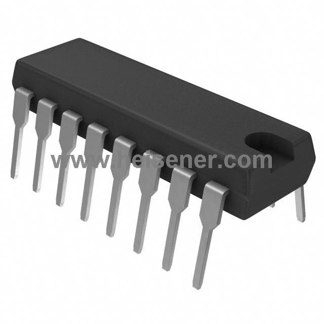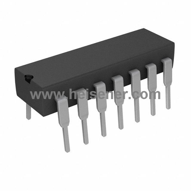
The LM324N is a quad operational amplifier integrated circuit housed in a 14-pin dual in-line plastic package (DIP-14). It contains four independent high-gain operational amplifiers. Key features include a wide supply voltage range of 3.0V to 32V, a true differential input stage, low quiescent current (typically 0.8mA), and a common-mode input range that extends to the negative power rail, making it suitable for both single-supply and dual-supply applications.
The LM324N operates on the principle of differential input and high-gain amplification characteristic of an operational amplifier. Inside the chip are four independent op-amp units, each with a differential input stage that can amplify the voltage difference of the input signal. It uses internal active components (transistors) and current mirror circuits to achieve stable current control and voltage amplification, producing an output signal that is proportional to or a result of an operation on the input.
The LM324N can be configured for various circuits, such as a voltage follower, inverting/non-inverting amplifier, integrator, or comparator. Its ability to operate on a wide range of power supply voltages and a common-mode input voltage that can go down to the negative supply rail makes it especially useful in single-supply applications.
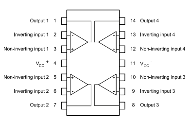
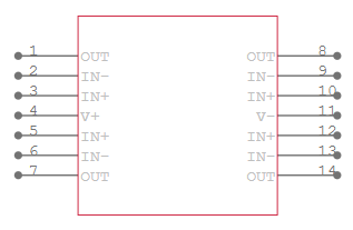
Output – The output terminal of operational amplifier.
Inverting Input – The inverting input of op-amp, where the signal enters with a 180° phase shift relative to the non-inverting input.
Non-inverting Input 1 – The non-inverting input of op-amp, where the signal enters without phase inversion.
VCC+ – Positive supply voltage pin.
VCC− (GND) – Negative supply voltage pin or ground reference. In single-supply mode, this is usually connected to 0V.
| Parameter | Value |
| Number of Circuits |
4 |
| Slew Rate | 0.4V/µs |
| Gain Bandwidth Product | 1.3 MHz |
| Input Offset Voltage | 2 mV |
| Input Bias Current | 20 nA |
| Supply Current | 1.5mA |
| Output / Channel Current | 40 mA |
| Supply Span Voltage | 3 V ~ 30V |
| Operating Temperature | 0°C ~ 70°C |
| Package | 14-DIP |
Wide gain bandwidth: 1.3 MHz
Input common mode voltage range includes ground
Large voltage gain: 100 dB
Very low supply current/amplifier: 375 µA
Low input bias current: 20 nA
Low input voltage: 3 mV max
Low input offset current: 2 nA
Wide power supply range:
-Single supply: 3 V to 30 V
-Dual supplies: ±1.5 V to ±15 V
Audio amplification
Sensor signal conditioning
DC motor speed control
Constant current source design
Voltage followers / buffers
Comparators
Active filters
Oscillator circuits
Analog computation
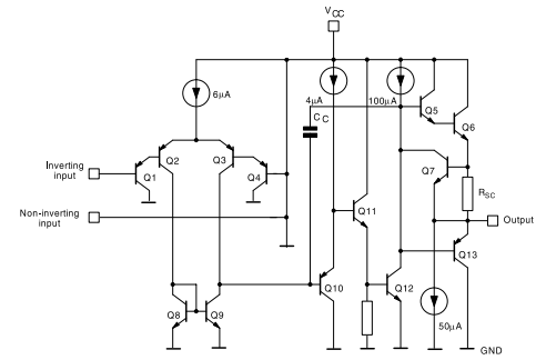
As we can see from the diagram, the internal circuit of the LM324N consists of a differential amplifier, a gain stage, and an output stage. The input stage is formed by transistors like Q1, Q2, Q3, and Q4, which amplify the voltage difference between the inverting and non-inverting inputs. A current source provides a constant current to ensure the input stage operates stably. Q8 and Q9 are used to bias the input stage, ensuring the symmetry of the differential input.
In the intermediate and output stages, Q10, Q11, and capacitor C form a compensation network. This improves the amplifier's stability and prevents oscillation. Components like Q5, Q6, Q7, Q12, and Q13 form a push-pull output structure, providing a higher drive capability. An output current source and a current-limiting resistor (Rsc) protect the circuit from overload. This overall structure ensures the LM324N has low power consumption, good stability, and high linearity across a wide range of supply voltages.
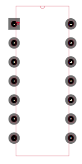
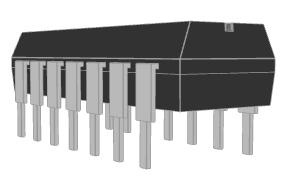
The 14-DIP (Dual In-line Package) is a common type of integrated circuit package featuring two parallel rows of pins, with a total of 14 pins. It is typically used for small logic chips, operational amplifiers, or timers. The pins have a standard spacing of 2.54 mm, making it easy to insert into a breadboard or solder onto a through-hole PCB. The package has a flat, rectangular shape, providing effective heat dissipation and convenient manual or automated installation.
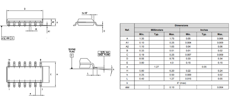
LM324AD: This is a pin-compatible alternative to the LM324N quad operational amplifier. It shares similar specifications such as low input offset voltage, low bias current, and a wide supply voltage range, making it suitable for applications like audio amplification, sensor signal conditioning, and DC motor control.
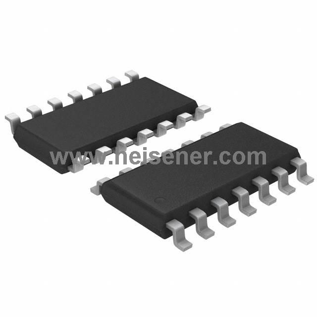
LM324DR: Functionally equivalent to the LM324N, the LM324DR provides the same four high-gain, frequency-compensated op-amps but typically comes in a SOIC-14 surface-mount package. It’s ideal for PCB designs requiring compact SMD installation while maintaining the same electrical performance.
LM324N is a quad operational amplifier IC with four independent op-amps in a single 14-DIP package, widely used in analog signal processing.
Yes, both are pin-compatible alternatives. LM324AD is similar in specifications, while LM324DR is usually an SMD SOIC-14 package version.
No, LM324N is a low-speed op-amp with limited slew rate (~0.5 V/µs), so it’s better for general-purpose analog circuits.