With the continuous development of cloud computing, ultra-large-scale data centers, 5G applications and large-scale equipment, the market demand for uninterruptible power supply (UPS) remains high, and is developing towards miniaturization, high capacity, and high efficiency. In the challenge of trade-offs between performance, energy efficiency, size, cost, and control difficulty, ON Semiconductor's solutions based on the next-generation semiconductor material silicon carbide (SiC) help to transformatively optimize UPS designs.
ON Semiconductor is one of the leading suppliers of smart power solutions and one of the few global suppliers of end-to-end SiC solutions from substrate to module, offering advanced SiC, SiC/Si hybrid and IGBT module technologies, as well as a wide range of discrete Devices, gate drivers and other peripheral devices meet the various requirements of low, medium and high power UPS design, and the application support of the technical team helps designers solve the above challenges and meet the growing demand in the era of big data. This article focuses on ON Semiconductor's SiC solution for UPS.
Online UPS is more suitable for high-power application scenarios
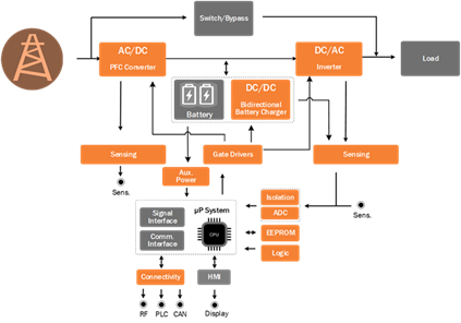
UPS systems are widely used to protect the power supply of critical components in a variety of applications ranging from telecommunications and data centers to various industrial facilities, providing filtering functions and compensating for short-term power outages in the grid, ensuring a reliable voltage supply. According to the working principle, UPS is divided into offline UPS, online interactive UPS and online UPS. Offline UPS and online interactive UPS have simple structure and low cost. In the case of no abnormal input, the energy efficiency is high, but there is a long switching time, many cases of activating battery power supply, and low output accuracy. Therefore, at present, online UPS is the most commonly used place for high-power UPS needs such as data centers. Online UPS is also called double conversion UPS. Regardless of whether the mains is normal or not, all the power of the load is given by the inverter. Therefore, there is no interruption, and the output quality is high. After high-frequency pulse width modulation (PWM), the overall waveform total harmonic distortion (THD) is small, and the frequency fluctuation is small, but the price is high and the control is complicated.
Design Challenges and Considerations for Next-Generation UPS
In order to cope with the growing demand for power protection, the new generation of UPS needs to have the following characteristics:
• Over 98% high energy efficiency, high power density, power factor >0.99, transformerless design
• Higher output power: Large data centers have high requirements on UPS. The bus voltage of a 3-phase output UPS is 800 V. Modular UPS is scalable, highly redundant, and can reach a maximum output power of 100 kVA by connecting multiple products to meet the needs of large data centers
• 0 switching time: Compared to the 2 to 10 ms switching time of offline UPS, online UPS has 0 switching time to deal with emergency problems in various situations
• Ability to adjust input voltage and optimize output voltage to reduce battery usage frequency, thereby increasing usage time and saving costs
• Excellent heat dissipation capability, reducing the weight and cost caused by the heat sink itself, while having the ability to add additional power modules in a limited space
In order to achieve these features, we need to balance the following factors:
• Control the Total Cost of Ownership (TCO, Total Cost of Ownership), including production costs, transportation, installation and post-maintenance costs, as well as space costs for storing equipment. Consider how to reduce the space and weight occupied by heat sinks, inductors and electrolytic capacitors, and fans.
• The scalability of UPS. One of the great advantages of modular UPS is scalability. When the capacity needs to be increased, only one power module needs to be added. One module is small in size and weight. Even one person can complete the installation, which greatly reduces the cost. .
• Adopt online UPS. Compared with other types of UPS, online UPS can handle more input power quality problems and reduce battery usage frequency. At the same time, its high-frequency inverter can output high-quality and high-efficiency sinusoidal signals to supply power to the load.
• The impact of topology on system performance and energy efficiency, 3-level topology is more energy efficient than 2-level topology, at rated power, higher energy efficiency means smaller heat sink and better reliability, the most critical is the electrical The increase of the average number makes the voltage output closer to a sine wave, but the complex control algorithm, more components and the increase in the number of switches will lead to an increase in cost, and designers need to make a trade-off between performance and price.
• Use SiC as switching device.
ON Semiconductor's SiC Solution for UPS: Wide Lineup and Excellent Performance
Since SiC has higher withstand voltage capability, lower losses and higher thermal conductivity, it can enable UPS design with higher power density and optimized system cost, lower system loss and higher system energy efficiency. ON Semiconductor has a deep history in the SiC field, and its vertical integration model ensures reliable quality and supply.
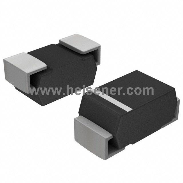
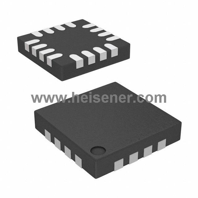
ON Semiconductor's extensive product line of SiC MOSFETs and SiC diodes includes various voltage levels. SiC MOSFETs are available from 650 V to 1200 V, and 1700 V products are coming soon, and SiC diodes are available from 650 V to 1700 V. For UPS, SiC MOSFET mainly chooses products with smaller Rdson. For example, ON Semiconductor's 1200 V M3S SiC MOSFET for UPS reduces power loss by up to 20% compared to industry-leading competitors because it uses a larger die, which reduces Rdson.
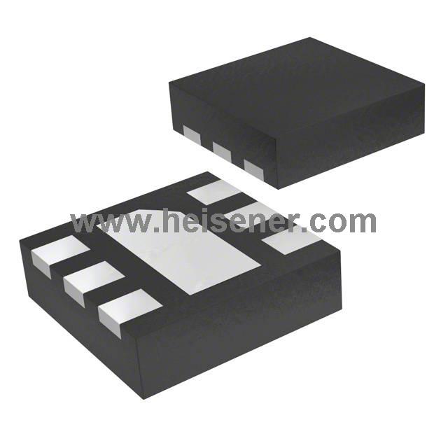
ON Semiconductor's current 4-pin SiC MOSFET, compared with 3-pin products, an additional Kelvin pin (Kelvin Source) can eliminate the parasitic inductance on the source pin, which can provide faster switching speed, thereby Reduce conduction losses.
As the unit power of the UPS gradually increases, more designers will consider module products. Many wafers with different functions and sizes, such as IGBTs and diodes, are packaged in one module, which can reduce the cost caused by single-tube pins. The stray inductance reduces the voltage stress generated by the device when the device is rapidly turned off, reduces the process of the production process, improves the efficiency of the production line, reduces the workload of the electrical and structural R&D designers, and avoids the product caused by the complex single-tube process. The defect rate also simplifies the procurement and supply chain of BOM, and shortens the time for products to be put into the market. And from the perspective of system integration, the high cost of the module can be diluted by other advantages, such as simplified production process and PCB design, high power density, lower heat dissipation system cost, simple insulation design, etc. Since the wafers used in assembling modules are all from adjacent devices on the same wafer, the consistency of the wafers is higher, which facilitates parallel current sharing of the wafers and increases the long-term operational reliability of the system.
ON Semiconductor's half-bridge 1200 V SiC MOSFET 2-PACK module contains 2 1200 V M1 SiC MOSFETs and a thermistor, with very low Rdson. It has 2 kinds of packages. The size of the F2 package NXH006P120MNF2 is twice that of the F1 package NXH010P120MNF1, which is more suitable for high-power products. At the same time, a larger die can reduce thermal resistance and increase the current that can be passed. ON Semiconductor's 900 V M2 SiC MOSFET Vienna module NXH020U90MNF2 consists of two 900 V switches and two 1200 V SiC diodes. The Vienna topology is often used in PFC. Compared with other 3-level solutions, the Vienna topology has fewer components and simple control. Features.
In addition, ON Semiconductor's multi-channel SiC boost module series is shown in the table below, which can be used for battery charging and discharging.
Loss comparison of different modules
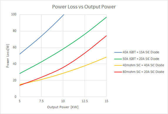
We compared different modules in a boost booster circuit, the SiC MOSFET's turn-on loss is 1 to 2 times lower than the IGBT hybrid module, and its turn-off loss Eoff is more than 5 times lower. This is of great significance for increasing the switching frequency of the system and reducing losses. Under the same switching frequency, the temperature rise and loss of the full SiC module are lower than that of the hybrid module, allowing the use of a smaller and more economical heat sink, or higher power output under the same heat dissipation conditions. Another evaluation method, assuming that the output power of each channel is 10 kW, with the increase of switching frequency, due to the larger switching loss, the junction temperature loss of IGBT is much higher than that of SiC MOSFET, so the full SiC module is reducing the inductance value and inductance value. There are huge advantages in terms of size and weight.