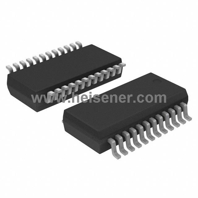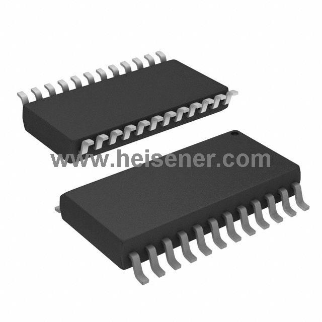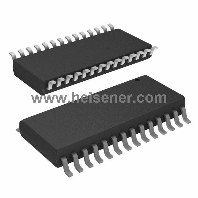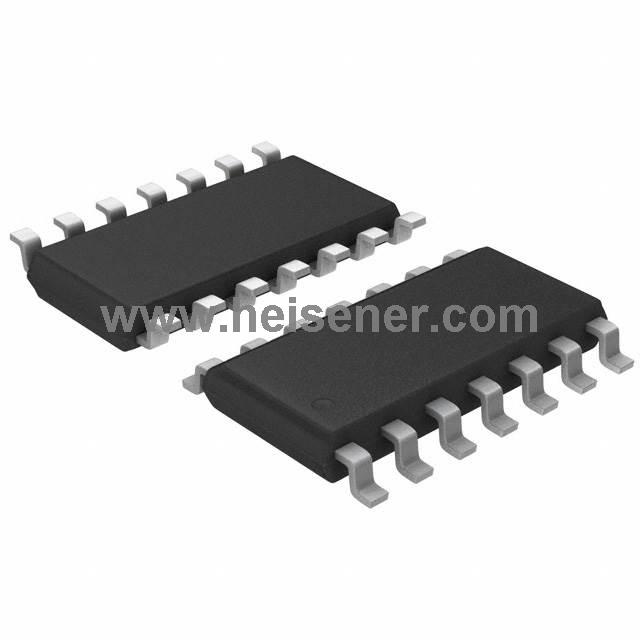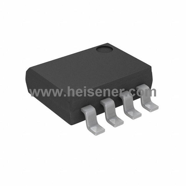
The SP3485 device is a 3.3V low-power half-duplex transceiver that meets the specifications of the RS-485 and RS-422 serial protocols. This device is pin-to-pin compatible with the MaxLinear SP481, SP483 and SP485 devices as well as popular industry standards. The SP3485 can meet the electrical specifications of the RS-485 and RS422 serial protocols up to 10Mbps under load.
The SP3485EN-L/TR transceiver uses differential signaling technology to facilitate long-distance data exchange.
In transmit mode, it converts single-ended TTL logic levels output by a controller into a pair of differential signals (lines A and B), defining the logic state based on the voltage difference between the two lines (VA - VB).
In receive mode, its internal high-sensitivity differential receiver detects minute voltage differences on the bus (typically with a threshold of ±200 mV) and restores them to standard TTL levels for output to the MCU.
Furthermore, the chip features DE (Driver Enable) and RE (Receiver Enable) control pins, allowing the system to rapidly switch between transmit and receive states, so it's ideally suited for multi-node industrial bus environments.
| Parameter | Specification |
| Model | SP3485EN-L/TR |
| Device Type | Transceiver |
| Protocol Support | RS-485 / RS-422 |
| Supply Voltage | 3V ~ 3.6V |
| Data Rate | 10 Mbps |
| Duplex | Half |
| Receiver Hysteresis | 20 mV |
| Bus Interface | Differential Bus |
| ESD Protection | Integrated Protection |
| Operating Temperature | -40°C ~ 85°C |
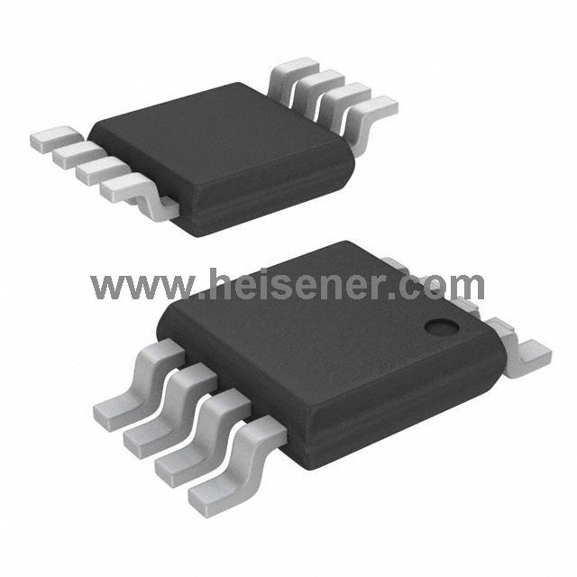
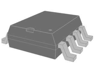
| Package | 8-SOIC |
| Mounting Type | Surface Mount |
| Base Product Number | SP3485 |
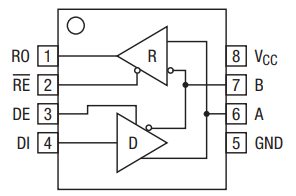
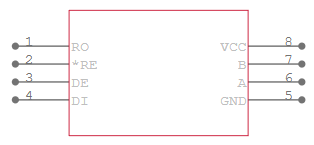
Pin 1 - RO: Receiver output
Pin 2 - RE: Receiver output enable active LOW
Pin 3 - DE: Driver output enable active HIGH
Pin 4 - DI: Driver input
Pin 5 - GND: Ground connection
Pin 6 - A: Non-inverting driver output / receiver input
Pin 7 - B: Inverting driver output / receiver input
Pin 8 - VCC: Positive supply
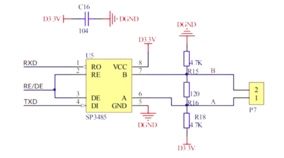
This SP3485 schematic shows a typical half-duplex RS-485 communication interface design. The RO and DI pins of transceiver U5 are directly connected to the MCU serial interface, while RE and DE are tied together, allowing fast switching between transmit and receive modes through a single RE/DE control line.
On the bus side, a 120Ω termination resistor is placed between the A and B lines to match impedance and reduce signal reflections. The circuit also uses 4.7KΩ pull-up and pull-down bias resistors (R15 connected to GND and R18 connected to 3.3V) to maintain a defined logic level when the bus is idle. In addition, capacitor C16 (104) provides power supply decoupling, helping ensure stable data transmission under the 3.3V supply.
| Features | Description |
| RS-485 / RS-422 Transceiver | Supports differential serial communication based on RS-485 and RS-422 standards |
| Single 3.3V Supply Operation | Operates from a single 3.3V power supply for low-power system designs |
| 5V Logic Compatible | Can interface directly with 5V logic systems |
| Driver and Receiver Enable Control | Supports independent transmit and receive mode switching |
| Wide Common-Mode Input Range | Supports -7V to +12V common-mode voltage for improved noise tolerance |
| Supports 32 Bus Nodes | Allows up to 32 transceivers on the same RS-485 communication bus |
| Industry-Standard Pinout Compatibility | Compatible with the standard 75176 pin configuration for easy replacement |
| Short-Circuit Protection | Integrated driver output short-circuit protection improves reliability and safety |
SP3485EN-L/TR Applications
| Applications | Examples | Benefits |
| Industrial Automation | PLC systems, industrial controllers, factory equipment | Reliable long-distance communication with strong noise immunity |
| Embedded Systems | MCU communication networks, embedded control boards | Low-power operation and simple UART interface integration |
| Building Automation | Smart lighting, HVAC control systems | Stable multi-device communication over a shared bus |
| Security Systems | Access control panels, surveillance equipment | Supports robust data transmission in electrically noisy environments |
| Communication Equipment | RS-485 serial converters, data acquisition systems | High-speed differential communication up to 10Mbps |
| Smart Metering | Energy meters, remote monitoring terminals | Enables long-range and multi-node network connectivity |
| Automotive Electronics | In-vehicle communication modules, diagnostic tools | Wide common-mode voltage range improves signal stability |
| IoT and Sensor Networks | Distributed sensor nodes, environmental monitoring systems | Supports up to 32 transceivers on a single communication bus |
SP3485EN-L/TR Equivalents
Common alternative models for the SP3485EN-L/TR include the MAX3485, SN65HVD3082E, ADM3485, ISL3170, SP485E, and LTC1480, among others.
Testing the SP3485EN-L/TR mainly involves two steps: static voltage measurement and dynamic communication testing. First, power on the circuit and use a multimeter to verify that the VCC pin (Pin 8) has a stable 3.3V supply and that the GND connection is correct. Then, switch modes by driving the RE/DE control line high or low and observe the voltage difference between the A and B bus lines. When transmitting logic "1", the A line voltage should be higher than B; when transmitting logic "0", the opposite should occur. If the idle-state differential voltage remains above 200mV, the bias circuit is working properly.
Next, perform a loopback or communication test to verify functionality. A simple method is to connect the RO (receiver output) back to the MCU and send data through a serial terminal to check whether the returned characters are received correctly.
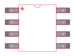
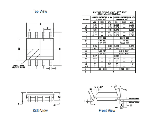
The following section primarily details the mechanical dimensions of the SP3485EN-L/TR, including its package outline, overall structural parameters, etc.
The SP3485 is a high-speed transceiver capable of data rates up to 10 Mbps. This makes it suitable for high-speed industrial fieldbus applications.
They control the receiver and driver enable functions, allowing switching between transmit and receive modes.
The primary difference is the supply voltage. The SP3485 operates at 3.3V, whereas the SP485 is the traditional 5V version.
SP3485EN-L/TR and other electronic parts are available from Heisener Electronics, a global distributor offering large in-stock inventory and fast delivery for OEMs, EMS providers, and electronics design companies.