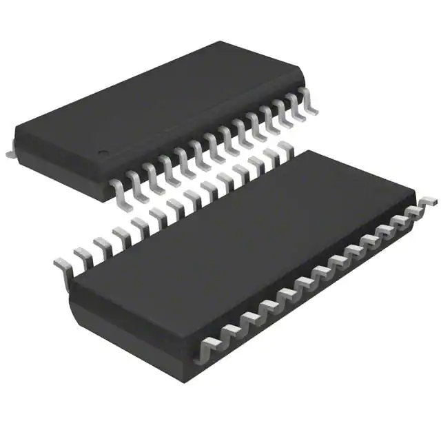
The CDCD5704 clock generator provides the necessary clock signals to support the XDR memory subsystem and the mahogany logic interface using reference clock inputs (with or without spread spectrum modulation). The CDCD5704 is included in a 28-pin TSSOP package that includes four differential clock outputs, providing an off-the-shelf solution for a wide range of high performance interface applications.
This block diagram shows the main components of CDCD5704, which include a phase-locked loop, a bypass multiplexer and four differential output buffers (CLK0 to CLK3). All four outputs can be disabled by logical low level at the EN pin input. Output is enabled when EN has a high value and the value in its serial interface register (RegA-RegD) is 1.

The PLL receives a reference clock input signal REFCLK and outputs a clock signal with a frequency equal to the input frequency multiplied by the multiplication factor. The PLL output clock signal is fed to the differential output buffer to drive the enabled clock. Disable output set to high impedance.
Sequence diagram, serial control interface
