Although semiconductor technology is booming today, there are still more devices and systems being produced using traditional power electronics systems. We must ensure that the manufacturing of various devices and technologies is sustainable, while keeping in mind different safety and environmental norms and improving efficiency.
With the introduction of wide band gap (WBG) devices such as silicon carbide (SiC) and gallium nitride (GaN), power electronics technology has undergone tremendous changes. In fact, the properties of these materials make them particularly suitable for applications that operate at high pressures and high switching frequencies, and can provide better efficiency and heat management than the most advanced silicon-based power devices.
PowerAmerica organized a wide band Gap semiconductor symposium on the theme "SiC and GaN: The Future is Now." Victor Veliadis, Executive Director and Chief Technology Officer of PowerAmerica, and other industry leaders spoke on the latest business and technology in SiC and GaN power semiconductors and applications.
PowerAmerica is a membership alliance of industry, universities and national laboratories whose goal is to accelerate the adoption of wide-band gap power electronics technology.
"Wide Band Gap companies cover the entire ecosystem, with many involved in SiC and GaN fabs and materials as well as devices, circuits and modules." "Then there are companies that manufacture industrial systems that basically plug silicon carbide into their systems and benefit from efficiency, weight reduction, small size and other advantages. We are also affiliated with many universities. In addition, we work closely with the White House and the Department of Energy to keep them informed of the expanding bandgap market. As a result, over the past three years, we have used $3.1 million in membership funds to complete 17 projects that were selected and executed by our members."
Dan Kinzer, co-founder and CTO/COO of Navitas Semiconductor, talks about the efficiency, reliability and autonomy of Gans. According to Navitas and other speakers, Gans and SiC are the future of the next power electronics revolution.
"We spend a lot of time in R&D, working with TSMC to develop our power devices and developing our process design suite." "Kinzer said.
Figure 1: GaN Opportunities.
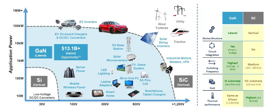
According to Navitas, SiC is an excellent solution for applications above 1,200V and 100kW, where horizontal GaN technology is more difficult to meet these power levels (Figure 1).
GaN solutions are horizontal and enable circuit integration. They can operate at very high switching frequencies. According to Navitas, GaN can reach up to 40MHz.
"It's certainly not a limitation of switching frequency - it's often some other system component, most likely magnetic, that becomes the key constraint." Kinzer points out.
"The advantage of GaN is the ability to form very thin films on silicon substrates." He added, "So it's a low-cost substrate that can be used in large quantities." There are also quite a few silicon fabs looking for migration strategies because Gans can use older generation semiconductor manufacturing techniques and equipment."
To get a thriving business and expand the reach of customers, you need to explore multiple markets. One of them is fast chargers, mainly below 300W, as this accounts for a large percentage of the approximately 60 million devices that have been sold so far. Companies such as Xiaomi have introduced 120W adapters that can charge a variety of devices faster than previous technologies.
From an environmental perspective, GaN devices can reduce CO2 emissions for electric vehicles by up to 2.5Gt per year.
"Along with all other uses, we are seeing the adoption of electric vehicles accelerating." Kinzer noted, "We are a certified carbon neutral company, and we are the first semiconductor manufacturer to achieve this certification. As a result, any carbon released during the production of our products has been offset. Monolithic integration has helped these results tremendously, and over time we expect to see integration pay off even more."
Wide band gap material
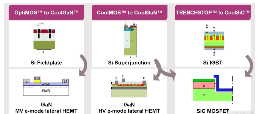
Peter Friedrichs, Vice President of Infineon Technologies, attended the conference as the keynote speaker. He noted that global megatrends, including digitization and decarbonization, require the use of wide bandgap devices such as SiC and GaN (Figure 2). Due to their special technical characteristics, they can provide maximum performance and energy efficiency at the same time.
"At the moment, we don't see a single power semiconductor application where wide bandgap won't have an impact on its timeline, it's not just an academic or technical activity." "Also, if you look at the megatrends that we're seeing today, we're really seeing tremendous growth, not only in electric vehicles, but also in a wide range of industrial applications, especially those that need to make electric vehicles operate like electric vehicle charging infrastructure or generating green electricity from renewable sources."
Figure 2: Infineon will complement each of its solutions with wide bandgap technology
Our analysis shows that solar power generation, EV charging, power supplies and uninterruptible power supplies (UPS) have reached or exceeded this tipping point." Friedrichs points out.
"We expect near-explosive growth in the use of silicon carbide from around 2025 as further applications increase dramatically, for example in electric vehicles, traction train propulsion or large-scale storage systems." "He added.
During the hot summer months, solar's share of the energy mix reached record levels. But what if there is no sunlight? Two-way charging makes it possible to store solar energy from photovoltaic systems in batteries in electric vehicles and homes and supply it back to the home grid at night or when household appliances need to be run. This approach allows us to protect the environment, save money, and will further incentivize our transition to emissions-free electric vehicles. Infineon and Delta Electronics have developed a three-in-one system that combines solar energy, energy storage and electric vehicle charging. Thanks to two-way inverters, electric vehicles can not only be charged, but also be used as buffer memory or family emergency backup power. More and more cars are equipped with this feature. Going forward, two-way energy flows can also be used to enable new vehicle-to-home and vehicle-to-grid solutions.
Today, we know very well what kind of impact we can have on the energy saving potential, but this is one of the applications that will really take time to move the industry from existing silicon-based platforms to SiC and motor-driven endpoints, which is also the largest part of industrial power electronics today.
Power density has now improved significantly, while overall losses associated with SiC semiconductor trading have been reduced by two-thirds. Friedrichs also points out that the noise level is also much lower, which is very important. This is especially important for residential applications or any installation close to a home. According to Friedrichs, UPS is another example of a product where the advantages of using SiC can be seen in operating expenses and installation costs.
Pavel Freundlich, Senior Director and CTO of onsemi's Power Solutions Group division, gave a keynote speech on the company's wide bandgap products.
onsemi focuses on the industrial and automotive sectors. The main goal of its industrial segment is to focus on energy storage and charging methods for solar conversion. On the automotive side, its main focus is on electric vehicle traction inverters using SiC.
"If we look at our own revenue, two-thirds of it comes from autos and industry." "Why autos and industrials? We believe they are the economic engines of the 21st century. This is why in the past, in the 20th century, the industry was characterized by energy concentration and the adoption of long-distance transmission and distribution, rather than very efficient consumption. As a result, energy comes mainly from fossil fuels, including gasoline-powered vehicles, internal combustion engines, and other high energy users. The result, of course, is carbon emissions. If global warming is to be limited to 1.5 ° C, we must act now. So it really is now or never, and our solutions are suitable for the automotive and industrial sectors. That's how we see the future. Instead of centralizing energy production, we switched to local renewable energy, which eliminated or significantly reduced long-distance power distribution and thus reduced the losses we suffered. And then, in terms of consumption, we have to be efficient, so we have to have efficient converters, efficient motors, and industrial automation."
As more and more automakers increase their investment in electric vehicle development, silicon carbide will become increasingly important to the automotive industry. It provides higher voltage, higher power density and higher efficiency. Each of these advantages helps to reduce cost per terminal, resulting in shorter charging times and longer charging intervals.
Figure 3: SiC leadership - from substrate to system
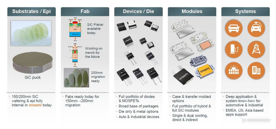
Figure 4: Electric vehicle charging station module
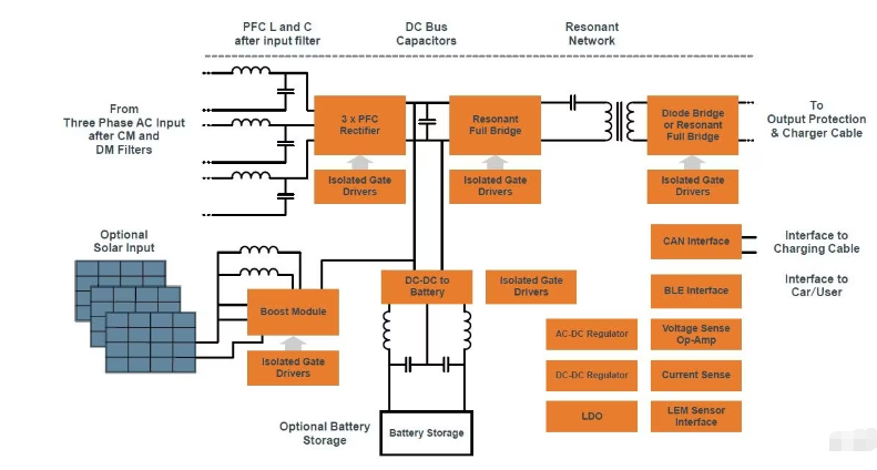
"Our silicon carbide solutions are suitable for all electric vehicle types across the market (Figure 3, Figure 4)." "In addition to traction inverters and electric vehicles, the solution can be applied to a wide range of use cases, such as AC/DC or DC/DC power converters, high-speed trains, photovoltaic inverters, medical devices, motor drives, grid transmission and solid-state transformers," Freundlich said.
Not only should we make longer-range electric vehicles the norm, but batteries should also be cheaper and charge faster if we want every car on the road to be electric. As silicon approaches its theoretical limits due to its larger band-gap width, stronger disruptive electric field, and higher thermal conductivity, the industry is turning to SiC for power electronics. Compared to silicon-based components, SIC-based MOSFETs have lower losses, higher switching frequencies, and higher power density.
SiC has strong physical bonding, which contributes to its excellent mechanical, chemical and thermal stability. However, manufacturing SiC wafers is a difficult process. Not every wafer is suitable for end products such as diodes and MOSFETs.
As a result, even though the industry has made great efforts to reach 200mm wafer diameters, a lot of emphasis has been placed on improving and optimizing the technology for 150mm wafers.
Even though there are still some challenges to address before 200mm wafers become the industry standard, the industry is already moving to larger diameter SiC wafers. SiC wafers are inherently more challenging to produce than silicon wafers of the same size.
Heisener Electronic is a famous international One Stop Purchasing Service Provider of Electronic Components. Based on the concept of Customer-orientation and Innovation, a good process control system, professional management team, advanced inventory management technology, we can provide one-stop electronic component supporting services that Heisener is the preferred partner for all the enterprises and research institutions.
